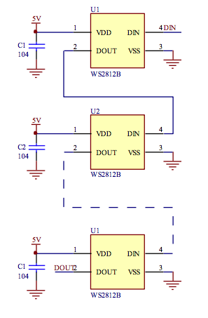
The WS281x (WS2811/WS2812) is an RGB LED control circuit allowing to configure (color, intensity) of multiple LEDs over one data line. The LEDs with the integrated WS281x circuit can be simply connected in serial using 3 lines (5V, GND and DATA).
The programing (configuring the colors) of the LED strip work s by sending 24bit (3 * 8bit for each color – RGB) packets over the data line. Since we have only one data line the timing is crucial here and also the biggest challenge, especially on resource-limited PICs.
There are two main approaches found on the internet. Software timing and hardware timing. The software timing puts a lot of pressure on the PIC itself. It needs a high frequency oscillator and fails often if the PIC does also other stuff than solely acting as a WS281x controller. Also on slower PIC (with lower frequency oscillators or high minimal instruction time) this task may be not possible.
The second approach is using some hardware peripherals of the PIC. There are some tutorials showing concrete examples but if you have a different PIC than in the examples you will still need to find some things out on your own.
Timing

As already mentioned the biggest challenge is the timing protocol of the WS281x. Since we have only one data line we have to rely on timing. The WS281x implements 3 timings: 0 code, 1 code and RET code. 0 code encodes a logical “0”, 1 code encodes a logical “1” and RET code encodes a reset sequence.
The period of a logical value is 1.25us (+/- 300ns). The 300ns tollerance is very important and a reason why the software approach fails very fast. A logical value always starts with high voltage time on the data line. The difference is for how long. In case of a logical “0” the T0H = 0.4us (+/- 150ns) and in case of a logical “1” the T1H = 0.8us (+/- 150ns). After a low voltage time follows on the data line filling the 1.25us period: in case of a logical “0” the T0L = 0.85us (+/- 150ns) and in case of logical “1” the T1L = 0.45us (+/- 150ns). Any low voltage signal over Treset = 50us is considered the RET code. See the datasheet for details.
What can be found is that there are some timings which needs to be held up precisely and some do not. The period is one of those timings which needs to be held up precisely. Mainly there must be no longer interruptions between codes due to the RET code. But the T0H/T0L and T1H/T1L ratio is a bit more open. One may say that if the high voltage part is longer than half of the period than it is considered as logical “1”, if the high voltage part is shorter than half of the period than its considered as logical “0”. This is an important observation when it comes to the implementation below.
Encoding
Encoding the color code of multiple LEDs works by sending a 24bit number for each LED over the data line. Lets say we have 10 LEDs in our strip. Look at the color order of the specific WS281x circuit. The one I was using uses the GRB order but this may differ.
We always start with low on the data line for more than 50us and by that sending the RET code. There is no limitation on how long we can stay in reset sequence. Therefore if no change is necessary we just leave the data line on low voltage.
The we sent 10 (LEDs) * 24 (8bit G + 8bit R + 8bit B) bits right after each other without any pauses (see timing above) setting every of the 10 LEDs in our strip. It is important that there are no pauses between the blocks since those may be considered RET codes and thereby reseting the sequence.
After we sent our data we leave the data line on low-voltage reseting the sequence. The LED will keep their configuration until a new configuration will be send.

The Hardware Approach
As discussed above we are considering only the hardware approach due to its reliability and lower requirements on the PIC. From multiple source I found regarding this issue the Application Notes AN1606 may be worth mentioning. It uses the PIC16F1509 but we will use only its generic parts.
To implement this approach you PIC needs to have free to use following 4 peripherals: a timer, PWM, CLC logic and a SPI interface. The idea is to send your data to the SPI interface and using the CLC logic with help of the PWM and timer to clock this data ones and zeros to the WS281x signal.
The SPI waveform looks like this:
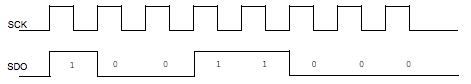
Over one full clock (SCK) period there is a logical “0” or logical “1” on the SDO data line. If we combine those 2 signals with a logical AND we get the following waveform:

If we consider our clock to be still SCK than in one period a logical “1” is now represented with approx. half the period high-voltage followed by half the period low-voltage. While a logical “0” is represented by low-voltage over the whole period. (I say approx. since there is raising and falling time to be considered)
Now we include a PWM as a short pulse generator with twice the frequency of the SPI interface:
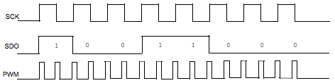
With a SCK & !SDO & PWM formula we can get the WS281x logical zeroes waveform:

Now we basically have the logical ones and logical zeroes on two different waveforms, what we need to do is to combine those into a single one:

And the resulting expression: (SCK & !SDO & PWM) | (SCK & SDO) we get the WS281x encoded waveform.
This way we represent a logical “1” by 1/2 period of high-voltage and 1/2 period of low-voltage. A logical “0” by 1/4 period of high-voltage and 3/4 period of low-voltage. Since the WS281x period is 1.25us than:
- Logical “1”: T1H = 625.0ns, T1L = 625.0ns
- Logical “0”: T0H = 312.5ns, T0L = 937.5ns
Which is not according to the WS281x datasheet but since the ration not the exact timing matters this works. Most probably because what matters is the T0H = 0.4us and the period = 1.25us from the datasheet. TxH <= T0H results into logical “0” and TxH > T0H results into logical “1”. This is just my assumption since I din’t find any such definition in the WS281x datasheet.
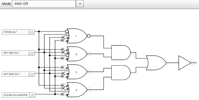
Configurable Logic Cell (CLC)
To implement this on the HW level we will use a CLC in AND-OR mode allowing us to combine up to 4 peripherals in a 4 * 4(N)OR + 2 * 2AND + 2OR circuit.
We will need to adapt the expression above to something implementable by this logic cell. We use the De Morgan laws and replace the first part (logical zeroes) as follows:
SCK & !SDO & PWM = (SCK & PWM) & !SDO = !(!SCK | !PWM) & !SDO
The resulting expression (!(!SCK | !PWM) & !SDO) | (SCK & SDO) can be then implemented in the CLC peripheral:
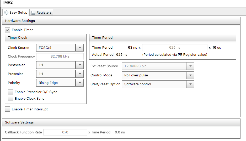
Timer Peripheral
Both the SPI interface and the PWM rely one timer. Take into consideration that the same timer needs to be used to the PWM and for the SPI and both the PWM and the SPI needs to be usable in one CLC. Your microcontroller may have some limitations on which of those peripherals may be used and connected to each other. Make sure you check those limitations.
In my case the timer needs to configure the clock source FOSC/4 in order to work with the PWM. Since the WS281x period is 1.25us and we need the PWM have twice the frequency out timer period needs to be 1.25us / 2 = 625ns.
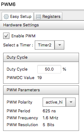
Pulse Width Modulator (PWM)
The PWM than should use this timer as a source with a duty cycle of 50%. Since the timer period is 625ns the PWM will generate a logical high of 625ns / 2 = 312.5ns which is also 1/4 of the WS281x’s period.
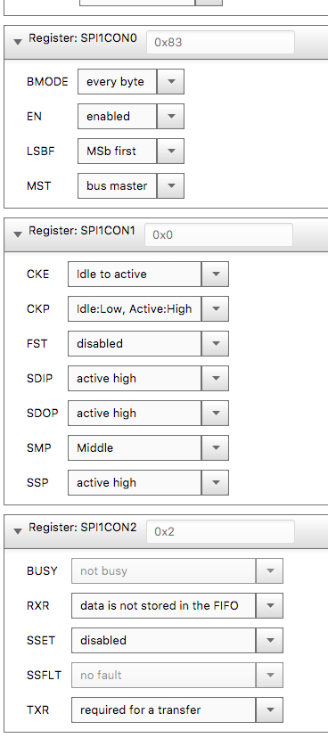
Serial Peripheral Interface (SPI)
The last thing to configure is the SPI interface. As a clock source use here also the same timer (TMR2_Postscaled in my case) and set clock divider to 0. Which should generate 800Mhz SPI Clock (half of the timers frequency).

If you are using a PIC with full SPI (non-MSSP) don’t forget to set BMODE to “every byte” and RXR to “data is not stored in the FIFO” or the corresponding register SPIxCON0 and SPIxCON2.
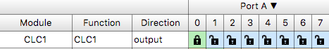
Connecting LED strip
The WS281x LED strip’s data line needs to be connected to the output of the CLC logic. In my case CLC1 output:
Software
In our example we want to be able to configure each LED separately. I was thinking about 5 different light patterns: light, blink, fade-in, fade-out and fade-toggle. The implementation provides a generic interface where the following parameters are considered for each LED: pattern, red-component, green-component, blue-component, delay, minimum and maximum value.
The program allows to operate in a simple-mode (without patterns) and pattern-mode. The pattern mode requires another timer which repeatedly triggers the update function. Ideally this timer’s period should be 10ms, 1ms or similar to allow smooth animation on one hand and not put too much load on the microcontroller.
One issue this implementation especially in the pattern-mode has is memory requirements. We need to load all the data which needs to be sent over the SPI interface to the CLC logic and the WS281x LED strip to memory. Considering the required parameters and the fact that a color-component needs to be stored twice (set value and current value), the memory usage of this module is depending on the number of LEDs: 2 * 3 (RGB) + 4 (pattern, delay, min, max) = 10bytes per LED. 50 LED strip will therefore need 500bytes of memory which may be too much for some PICs.
/*
 * File:   ws281x.h
 * Author: Jan Kubovy <jan@kubovy.eu>
 *
 * WS281x implementation. Needs WS281x_BUFFER to be defined to SPI transmission
 * buffer (e.g. SPI1TXB) and WS281x_LED_COUNT to be set to number of LEDs on the
 * strip.
 */
#include <stdbool.h>
#include <stdint.h>

#define WS281x_PATTERN_LIGHT 0x00       // Simple light
#ifdef WS281x_TIMER_PERIOD
#define WS281x_PATTERN_BLINK 0x01       // Blink 50/50
#define WS281x_PATTERN_FADE_IN 0x02     // Fade in 0>1
#define WS281x_PATTERN_FADE_OUT 0x03    // Fade out 1>0
#define WS281x_PATTERN_FADE_TOGGLE 0x04 // Fade toggle 0>1>0
#endif

uint8_t ledDataR[WS281x_LED_COUNT];
uint8_t ledDataG[WS281x_LED_COUNT];
uint8_t ledDataB[WS281x_LED_COUNT];
uint8_t ledTempR[WS281x_LED_COUNT];
uint8_t ledTempG[WS281x_LED_COUNT];
uint8_t ledTempB[WS281x_LED_COUNT];
uint8_t ledPattern[WS281x_LED_COUNT];
uint8_t ledDelay[WS281x_LED_COUNT];
uint8_t ledMin[WS281x_LED_COUNT];
uint8_t ledMax[WS281x_LED_COUNT];

uint16_t WS281x_counter = 0;

/**
 * Show/populate configuration buffer on WS281x LEDs
 */
void WS281x_show(void) {
    for (uint8_t i = 0; i < WS281x_LED_COUNT; i++) {
        WS281x_BUFFER = ledTempR[i];
        __delay_us(15);
        WS281x_BUFFER = ledTempG[i];
        __delay_us(15);
        WS281x_BUFFER = ledTempB[i];
        __delay_us(15);
    }
}

#ifdef WS281x_TIMER_PERIOD
/**
 * Update configuration buffer.
 *
 * This function should be called periodically by a timer. The timers period
 * should match WS281x_TIMER_PERIOD constant.
 */
void WS281x_update(void) {
    uint8_t percent;
    for (uint8_t led = 0; led < WS281x_LED_COUNT; led++) {
        switch(ledPattern[led]) {
            case WS281x_PATTERN_LIGHT:
                percent = 255;
                break;
            case WS281x_PATTERN_BLINK:
                percent = (WS281x_counter / ledDelay[led]) % 2
                        ? ledMax[led] : ledMin[led];
                break;
            case WS281x_PATTERN_FADE_IN:
                percent = (WS281x_counter / ledDelay[led]) % 100;
                percent = ((uint16_t) (ledMax[led] - ledMin[led]) * percent)
                        / 99  + ledMin[led];
                break;
            case WS281x_PATTERN_FADE_OUT:
                percent = (WS281x_counter / ledDelay[led]) % 100;
                percent = ledMax[led]
                        - ((uint16_t) (ledMax[led] - ledMin[led]) * percent)
                        / 99;
                break;
            case WS281x_PATTERN_FADE_TOGGLE:
                percent = (WS281x_counter / ledDelay[led]) % 200;
                percent = percent > 100 ? 200 - percent : percent;
                percent = (ledMax[led] - ledMin[led]) * percent / 100
                        + ledMin[led];
                break;
        }
        ledTempR[led] = ledDataR[led] * percent / 255;
        ledTempG[led] = ledDataG[led] * percent / 255;
        ledTempB[led] = ledDataB[led] * percent / 255;
    }
    WS281x_counter++;
    WS281x_show();
}
#endif

/**
 * Sets the given LED to specified color and pattern.
 *
 * @param led LED ID
 * @param pattern Pattern: WS281x_PATTERN_LIGHT, WS281x_PATTERN_BLINK,
 *                         WS281x_PATTERN_FADE_IN, WS281x_PATTERN_FADE_OUT, or
 *                         WS281x_PATTERN_FADE_TOGGLE
 * @param r Red color component
 * @param g Green color component
 * @param b Blue color component
 * @param delay Delay (pattern specific)
 * @param min Minimum value  (pattern specific)
 * @param max Maximum value  (pattern specific)
 */
void WS281x_set(uint8_t led, uint8_t pattern, uint8_t r, uint8_t g, uint8_t b,
                uint16_t delay, uint8_t min, uint8_t max) {
#ifdef WS281x_SW_LAT
    WS281x_SW_LAT = true;
#endif
    ledPattern[led] = pattern;

    ledDataR[led] = r;
    ledDataG[led] = g;
    ledDataB[led] = b;

    ledTempR[led] = r;
    ledTempG[led] = g;
    ledTempB[led] = b;

#ifdef WS281x_TIMER_PERIOD
    ledDelay[led] = delay / WS281x_TIMER_PERIOD;
#endif
    //ledCounter[led] = 0;

    ledMin[led] = min;
    ledMax[led] = max;
    WS281x_show();
}

/**
 * Turns WS281x LED strip off.
 */
void WS281x_off(void) {
    for (uint16_t led = 0; led < WS281x_LED_COUNT; led++) {
        WS281x_RGB(led, 0x00, 0x00, 0x00);
    }
    WS281x_show();
#ifdef WS281x_SW_LAT
    WS281x_SW_LAT = false;
#endif
}
The full code can be found under the following links: https://github.com/kubovy/mclib/blob/master/modules/ws281x.h, https://github.com/kubovy/mclib/blob/master/modules/ws281x.c
Hi, and thank you for the post.
I further went down the de morgan way and found out, that the whole expression of “(SCK & !SDO & PWM) | (SCK & SDO)” is realized using just 3 NAND gates. I made driver using a SPI and PWM on a STM8S and a single 74HC00 logic (4 NANDs). to describe it here in this comment, I write a nand as a “nand(a,b)”:
nand( nand(sck,sdo) , nand(sck,pwm) ).
that’s wonderfully ez and straight forward. one gate has sck,pwm inputs, the other one has sck,sdo inputs. both outputs go to the inputs of the third gate and the output is readilly usable. no additional inverters are used; even the PWM is not negated.
I’ve tested it and it works perfectly.